Our design goal is to eliminate the need for nop instructions.
The design method is to detect the need for a nop and stall
the IF and ID stages of the pipeline, inserting a nop into
the execution stage instruction register, EX_IR.
The initial instruction sequence was:
400 lw $1,100($0) load general register 1 from memory location 100
404 lw $2,104($0) load general register 2 from memory location 104
408 nop
40C nop wait for register $2 to get data
410 add $3,$1,$2 add contents of registers 1 and 2, sum into register 3
414 nop
418 nop wait for register $3 to get data
41C add $4,$3,$1 add contents of registers 3 and 1, sum into register 4
420 nop
424 nop wait for register $4 to get data
428 beq $3,$4,-100 branch if contents of register 3 and 4 are equal to 314
42C add $4,$4,$4 add ..., this is the "delayed branch slot" always exec.
The pipeline stage table with data forwarding and automatic hazard
elimination reduces to:
400 lw $1,100($0) IF ID EX M WB
404 lw $2,104($0) IF ID EX M WB
408 add $3,$1,$2 IF ID ID EX M WB
--
40C add $4,$3,$1 IF IF ID EX M WB
410 beq $3,$4,-100 IF ID ID EX M WB
414 add $4,$4,$4 IF IF ID EX M WB
time 1 2 3 4 5 6 7 8 9 10 11 12
(actually clock count)
Note that the -- indicates that IF stage and ID stage have stalled.
The -- also indicates a nop instruction has automatically been
inserted into the EX stage.
A new instruction can not move into the ID stage when an instruction
is stalled there. A new instruction can not move into the IF stage
when an instruction is stalled there. No column may have more than
one instruction in each stage. Any unlisted stage has a nop.
The compiler may now generate compressed code for the computer
architecture, saving on memory bandwidth because nop instructions
are not needed in the executable memory image. (Except a rare nop
instruction after a branch or jump instruction.)
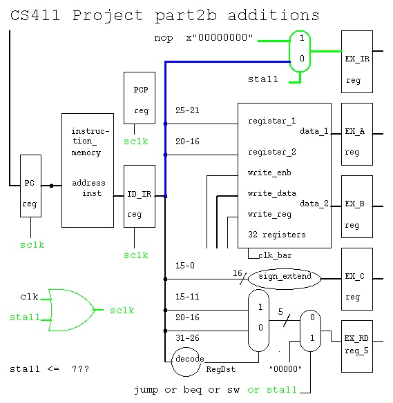
The primary task will be the implementation of a "stall" signal
for the project part2b.vhdl. The "stall" signal will then be used
to prevent clocking of the instruction fetch, IF stage and
instruction decode, ID stage by using a new clock signal "sclk".
The explanation for generating "sclk" is presented below.
Note that when the nop instruction is muxed into EX_IR then
the EX_RD must be set to zero along with the existing beq, sw and jump.
The changes in part2b.vhdl are in the IF and ID stages.
Green must be added. The signal "stall" is computed from the
information presented below.
 A "hazard" is a condition in the pipeline when a stage of the pipeline
would not perform the correct processing with the available data.
To be a hazard, the action of data forwarding, covered in the previous
lecture, must be taken into account.
Some cases where hazards would occur are:
lw $1,100($0)
add $2,$1,$1
EX stage MEM stage
add $2,$1,$1 lw $1,100($0) hazard!
value for $1 not available
Thus hold add $2,$1,$1 in ID stage, insert nop in EX, this is a stall.
ID stage EX stage MEM stage
add $2,$1,$1 nop lw $1,100($0) no hazard
ID stage EX stage MEM stage WB stage
add $2,$1,$1 nop lw $1,100($0) no hazard
| | |
+--+-------------------+ data forwarding
add $4,$3,$1
beq $3,$4,-100
ID stage EX stage
beq $3,$4,-100 add $4,$3,$1 hazard!
value for $4 not available
ID stage EX stage MEM stage
beq $3,$4,-100 nop add $4,$3,$1 no hazard
| |
+---------------------------------+ data forwarding
lw $5,40($1)
beq $5,$4,L2
ID stage EX stage
beq $5,$4,L2 lw $5,40($1) hazard!
value for $5 not available
ID stage EX stage MEM stage
beq $5,$4,L2 nop lw $5,40($1) hazard!
value for $5 not available
ID stage EX stage MEM stage WB stage
beq $5,$4,L2 nop nop lw $5,40($1) no hazard
| |
+------------------------------------------+ normal lw
Cases for stall hazards (taking into account data forwarding)
based on cs411 schematic. This is NOT VHDL, just definitions.
Note: ( OP stands for opcode, bits (31 downto 26)
lw stands for load word opcode "100011"
addi stands for add immediate opcode "001111" etc.
rr_op stands for OP = "000000" )
lw $a, ...
op $b, $a, $a where op is rr_op, beq, sw
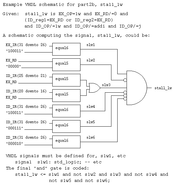
stall_lw is EX_OP=lw and EX_RD/=0 and
(ID_reg1=EX_RD or ID_reg2=EX_RD)
and ID_OP/=lw and ID_OP /=addi and ID_OP/=j
(note: the above handles the special cases where
sw needs both registers. sll, srl, cmpl have a zero in unused register.
no stall can occur based on EX_RD, MEM_RD or WB_RD = 0)
lw $a, ...
lw $b,addr($a) or addi $b,addr($a)
stall_lwlw is EX_OP=lw and EX_RD/=0 and
(ID_OP=lw or ID_OP=addi) and
ID_reg1=EX_RD
lw $a ...
beq $a,$a, ...
stall_mem is ID_OP=beq and MEM_RD/=0 and MEM_OP=lw and
(ID_reg1=MEM_RD or ID_reg2=MEM_RD)
op $a, ... where op is rr_op and addi
beq $a,$a, ...
stall_beq is ID_OP=beq and EX_RD/=0 and
(ID_reg1=EX_RD or ID_reg2=EX_RD)
ID_RD is 0 for ID_OP= beq, j, sw, stall (nop automatic zero)
thus EX_RD, MEM_RD, WB_RD = 0 for these instructions
rr_op is "000000" for add, sub, cmpl, sll, srl, and, mul, ...
stall is stall_lw or stall_lwlw or stall_mem or stall_beq
Be sure to use this semesters cs411_opcodes.txt, it changes every semester.
cs411_opcodes.txt for op codes
An partial implementation of stall_lw is:
A "hazard" is a condition in the pipeline when a stage of the pipeline
would not perform the correct processing with the available data.
To be a hazard, the action of data forwarding, covered in the previous
lecture, must be taken into account.
Some cases where hazards would occur are:
lw $1,100($0)
add $2,$1,$1
EX stage MEM stage
add $2,$1,$1 lw $1,100($0) hazard!
value for $1 not available
Thus hold add $2,$1,$1 in ID stage, insert nop in EX, this is a stall.
ID stage EX stage MEM stage
add $2,$1,$1 nop lw $1,100($0) no hazard
ID stage EX stage MEM stage WB stage
add $2,$1,$1 nop lw $1,100($0) no hazard
| | |
+--+-------------------+ data forwarding
add $4,$3,$1
beq $3,$4,-100
ID stage EX stage
beq $3,$4,-100 add $4,$3,$1 hazard!
value for $4 not available
ID stage EX stage MEM stage
beq $3,$4,-100 nop add $4,$3,$1 no hazard
| |
+---------------------------------+ data forwarding
lw $5,40($1)
beq $5,$4,L2
ID stage EX stage
beq $5,$4,L2 lw $5,40($1) hazard!
value for $5 not available
ID stage EX stage MEM stage
beq $5,$4,L2 nop lw $5,40($1) hazard!
value for $5 not available
ID stage EX stage MEM stage WB stage
beq $5,$4,L2 nop nop lw $5,40($1) no hazard
| |
+------------------------------------------+ normal lw
Cases for stall hazards (taking into account data forwarding)
based on cs411 schematic. This is NOT VHDL, just definitions.
Note: ( OP stands for opcode, bits (31 downto 26)
lw stands for load word opcode "100011"
addi stands for add immediate opcode "001111" etc.
rr_op stands for OP = "000000" )
lw $a, ...
op $b, $a, $a where op is rr_op, beq, sw
stall_lw is EX_OP=lw and EX_RD/=0 and
(ID_reg1=EX_RD or ID_reg2=EX_RD)
and ID_OP/=lw and ID_OP /=addi and ID_OP/=j
(note: the above handles the special cases where
sw needs both registers. sll, srl, cmpl have a zero in unused register.
no stall can occur based on EX_RD, MEM_RD or WB_RD = 0)
lw $a, ...
lw $b,addr($a) or addi $b,addr($a)
stall_lwlw is EX_OP=lw and EX_RD/=0 and
(ID_OP=lw or ID_OP=addi) and
ID_reg1=EX_RD
lw $a ...
beq $a,$a, ...
stall_mem is ID_OP=beq and MEM_RD/=0 and MEM_OP=lw and
(ID_reg1=MEM_RD or ID_reg2=MEM_RD)
op $a, ... where op is rr_op and addi
beq $a,$a, ...
stall_beq is ID_OP=beq and EX_RD/=0 and
(ID_reg1=EX_RD or ID_reg2=EX_RD)
ID_RD is 0 for ID_OP= beq, j, sw, stall (nop automatic zero)
thus EX_RD, MEM_RD, WB_RD = 0 for these instructions
rr_op is "000000" for add, sub, cmpl, sll, srl, and, mul, ...
stall is stall_lw or stall_lwlw or stall_mem or stall_beq
Be sure to use this semesters cs411_opcodes.txt, it changes every semester.
cs411_opcodes.txt for op codes
An partial implementation of stall_lw is:
 To check on the "stall" signal, you may need to add:
prtstall: process (stall)
variable my_line : LINE; -- my_line needs to be defined
begin
write(my_line, string'("stall="));
write(my_line, stall); -- or hwrite for long signals
write(my_line, string'(" at="));
write(my_line, now); -- "now" is simulation time
writeline(output, my_line); -- outputs line
end process prtstall;
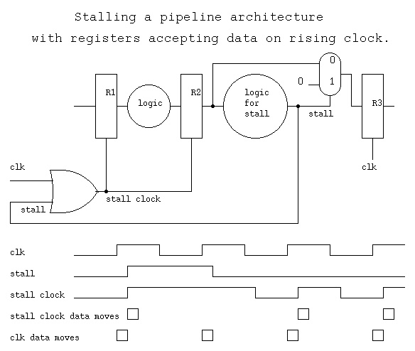
stall clock, sclk, is:
for raising edge registers clk or stall (our circuit)
To check on the "stall" signal, you may need to add:
prtstall: process (stall)
variable my_line : LINE; -- my_line needs to be defined
begin
write(my_line, string'("stall="));
write(my_line, stall); -- or hwrite for long signals
write(my_line, string'(" at="));
write(my_line, now); -- "now" is simulation time
writeline(output, my_line); -- outputs line
end process prtstall;
stall clock, sclk, is:
for raising edge registers clk or stall (our circuit)
 For checking your results:
part2b.chk look for inserted nop's
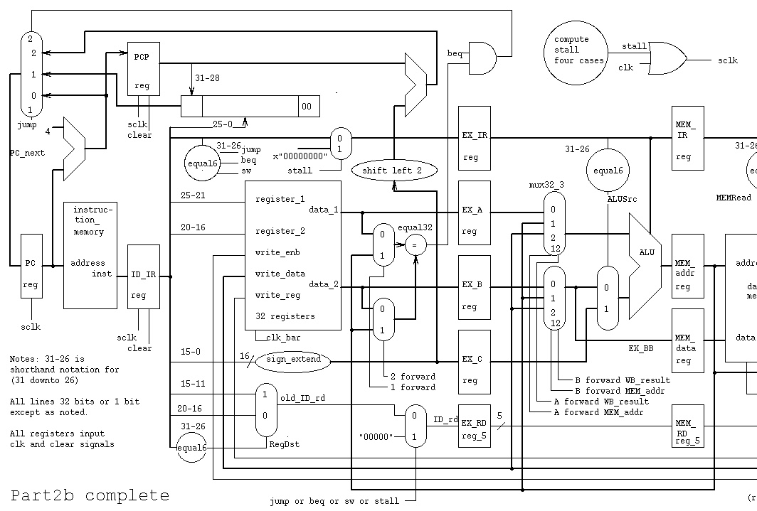
part2b.jpg complete schematic as jpeg image
part2b.ps complete schematic as postscript image
Project writeup part2b
Why is eliminating nop from the load image important?
Answer: memory bandwidth. RAM memory has always been slower than
the CPU. Often by a factor of 10. Thus, the path from RAM memory
into the CPU has been made wide. a 64 bit wide memory bus is
considered small today. 128 bit and 256 bit memory input to the
CPU is common.
Many articles have been written that say "adding more RAM to your
computer will give more performance improvement than adding a
faster CPU." This is often true because of the complex interaction
of the operating system, application software, computer architecture
and peripheral equipment. Adding RAM to most computers is easy and
can be added by non experts. The important step in adding more RAM
is to get the correct Dual Inline Memory Modules, DIMM's. There are
speed considerations, voltage considerations, number of pins and
possible pairing considerations. The problem is that there are
many choices. The following table indicates some of the choices yet
does not include RAM size.
Type Memory Symbol Module DIMM Nominal Memory
Bus Bandwidth Pins Voltage clock
DDR3 1600Mhz PC3-12800 12.8GT/sec 240 1.6 volt 200Mhz
38.4GB/sec may
DDR3 1333Mhz PC3-10600 10.7GT/sec 240 1.6 volt 166Mhz triple
DDR3 1066Mhz PC3-8500 8.5GT/sec 240 1.6 volt 133Mhz channel
DDR3 800Mhz PC3-6400 6.4GT/sec 240 1.6 volt 100Mhz (10ns)
DDR2 1066MHz PC2-8500 17.0GB/sec 240 2.2 volt two channel
DDR2 1000MHz PC2-8000 16.0GB/sec 240 2.2 volt
DDR2 900MHz PC2-7200 14.4GB/sec 240 2.2 volt
DDR2 800MHz PC2-6400 12.8GB/sec 240 2.2 volt
DDR2 667MHz PC2-5300 10.6GB/sec 240 2.2 volt
DDR2 533MHz PC2-4200 8.5GB/sec 240 2.2 volt
DDR2 400MHz PC2-3200 6.4GB/sec 240 2.2 volt
DDR 556MHz PC-4500 9.0GB/sec 184 2.6 volt
DDR 533MHz PC-4200 8.4GB/sec 184 2.6 volt
DDR 500MHz PC-4000 8.0GB/sec 184 2.6 volt
DDR 466MHz PC-3700 7.4GB/sec 184 2.6 volt
DDR 433MHz PC-3500 7.0GB/sec 184 2.6 volt
DDR 400MHz PC-3200 6.4GB/sec 184 2.6 volt
DDR 366MHz PC-3000 5.8GB/sec 184 2.6 volt
DDR 333MHz PC-2700 5.3GB/sec 184 2.6 volt
DDR 266MHz PC-2100 4.2GB/sec 184 2.6 volt
DDR 200MHz PC-1600 3.2GB/sec 184 2.6 volt
Pre DDR had 168 pin 3.3 volt DIMM's.
Older machines had 72 pin RAM
Then, there is the size of the DIMM in bytes.
(may need 2 DDR2 or 3 DDR3 in parallel, minimum 6GB DDR3)
128MB
256MB
512MB
1024MB 1GB
2048MB 2GB
4096MB 4GB
Then, there is a choice of NON-ECC or ECC, Error Correcting Code
that may be desired in commercial systems.
Then, possibly a choice of buffered or unbuffered.
Then, a choice of response CL3, CL4, CL5 clock waits.
(in detail may read 7-7-7-20 notation)
Then, shop by price or manufacturers history of reliability.
Some systems require DIMM's of the same size and speed be installed
in pairs. Read your computers manual or check for information on
WEB sites. I have uses the following sites to get information and
purchase more RAM.
www.crucial.com
You may search by your computers make and model, or by
DDR2 and see specification to find what is available.
www.kingston.com
www.kingston.com KHX8500
www.valueram.com/datsheets/KHX8500D2_1G.pdf
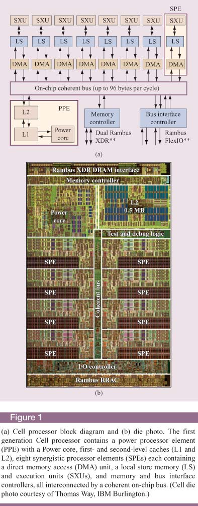
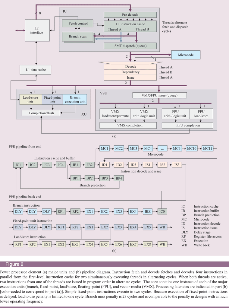
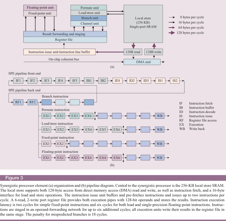
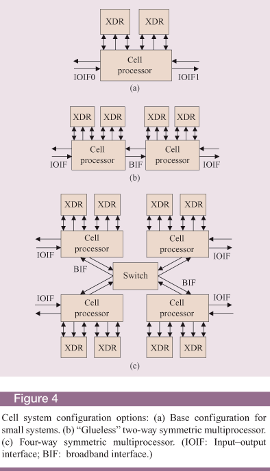
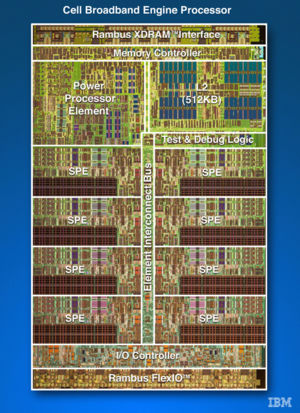
Now, how can an architecture best make use of the combination of
pipelines and memory. IBM Cell Processor uses an architecture of
a general purpose CPU on chip with eight additional pipeline
processors.
For checking your results:
part2b.chk look for inserted nop's
part2b.jpg complete schematic as jpeg image
part2b.ps complete schematic as postscript image
Project writeup part2b
Why is eliminating nop from the load image important?
Answer: memory bandwidth. RAM memory has always been slower than
the CPU. Often by a factor of 10. Thus, the path from RAM memory
into the CPU has been made wide. a 64 bit wide memory bus is
considered small today. 128 bit and 256 bit memory input to the
CPU is common.
Many articles have been written that say "adding more RAM to your
computer will give more performance improvement than adding a
faster CPU." This is often true because of the complex interaction
of the operating system, application software, computer architecture
and peripheral equipment. Adding RAM to most computers is easy and
can be added by non experts. The important step in adding more RAM
is to get the correct Dual Inline Memory Modules, DIMM's. There are
speed considerations, voltage considerations, number of pins and
possible pairing considerations. The problem is that there are
many choices. The following table indicates some of the choices yet
does not include RAM size.
Type Memory Symbol Module DIMM Nominal Memory
Bus Bandwidth Pins Voltage clock
DDR3 1600Mhz PC3-12800 12.8GT/sec 240 1.6 volt 200Mhz
38.4GB/sec may
DDR3 1333Mhz PC3-10600 10.7GT/sec 240 1.6 volt 166Mhz triple
DDR3 1066Mhz PC3-8500 8.5GT/sec 240 1.6 volt 133Mhz channel
DDR3 800Mhz PC3-6400 6.4GT/sec 240 1.6 volt 100Mhz (10ns)
DDR2 1066MHz PC2-8500 17.0GB/sec 240 2.2 volt two channel
DDR2 1000MHz PC2-8000 16.0GB/sec 240 2.2 volt
DDR2 900MHz PC2-7200 14.4GB/sec 240 2.2 volt
DDR2 800MHz PC2-6400 12.8GB/sec 240 2.2 volt
DDR2 667MHz PC2-5300 10.6GB/sec 240 2.2 volt
DDR2 533MHz PC2-4200 8.5GB/sec 240 2.2 volt
DDR2 400MHz PC2-3200 6.4GB/sec 240 2.2 volt
DDR 556MHz PC-4500 9.0GB/sec 184 2.6 volt
DDR 533MHz PC-4200 8.4GB/sec 184 2.6 volt
DDR 500MHz PC-4000 8.0GB/sec 184 2.6 volt
DDR 466MHz PC-3700 7.4GB/sec 184 2.6 volt
DDR 433MHz PC-3500 7.0GB/sec 184 2.6 volt
DDR 400MHz PC-3200 6.4GB/sec 184 2.6 volt
DDR 366MHz PC-3000 5.8GB/sec 184 2.6 volt
DDR 333MHz PC-2700 5.3GB/sec 184 2.6 volt
DDR 266MHz PC-2100 4.2GB/sec 184 2.6 volt
DDR 200MHz PC-1600 3.2GB/sec 184 2.6 volt
Pre DDR had 168 pin 3.3 volt DIMM's.
Older machines had 72 pin RAM
Then, there is the size of the DIMM in bytes.
(may need 2 DDR2 or 3 DDR3 in parallel, minimum 6GB DDR3)
128MB
256MB
512MB
1024MB 1GB
2048MB 2GB
4096MB 4GB
Then, there is a choice of NON-ECC or ECC, Error Correcting Code
that may be desired in commercial systems.
Then, possibly a choice of buffered or unbuffered.
Then, a choice of response CL3, CL4, CL5 clock waits.
(in detail may read 7-7-7-20 notation)
Then, shop by price or manufacturers history of reliability.
Some systems require DIMM's of the same size and speed be installed
in pairs. Read your computers manual or check for information on
WEB sites. I have uses the following sites to get information and
purchase more RAM.
www.crucial.com
You may search by your computers make and model, or by
DDR2 and see specification to find what is available.
www.kingston.com
www.kingston.com KHX8500
www.valueram.com/datsheets/KHX8500D2_1G.pdf
Now, how can an architecture best make use of the combination of
pipelines and memory. IBM Cell Processor uses an architecture of
a general purpose CPU on chip with eight additional pipeline
processors.
Monday, June 24, 2013
Pipeline Hazard and Stalls
Subscribe to:
Post Comments (Atom)
No comments:
Post a Comment