few definitions:
Pipelining : Multiple instructions being executed, each in a different
stage of their execution. A form of parallelism.
Super Pipelining : Advertising term, just longer pipelines.
Super Scalar : Having multiple ALU's. There may be a mix of some
integer ALU's and some Floating Point ALU's.
Multiple Issue : Starting a few instructions every clock.
The CPI can be a fraction, 4 issue gives a CPI of 1/4 .
Dynamic Pipeline : This may include all of the above and also can
reorder instructions, use data forwarding and
hazard workarounds.
Pipeline Stages : For our study of the MIPS architecture,
IF Instruction Fetch stage
ID Instruction Decode stage
EX Execute stage
MEM Memory access stage
WB Write Back into register stage
Hyper anything : Generally advertising terminology.
Consider the single cycle machine in the previous lecture.
The goal is to speed up the execution of programs, long sequences
of instructions. Keeping the same manufacturing technology, we can
look at speeding up the clock by inserting clocked registers at
key points. Note the placement of blue registers that tries to
minimize the gate delay time between any pair of registers.
Thus, allowing a faster clock.
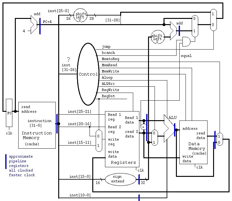 This is called approximate because some additional design must
be performed, mostly on "control", that must now be distributed.
The next step in the design, for our project, is to pass the
instruction along the pipeline and keep the design of each
stage of the pipeline simple, just driven by the instruction
presently in that stage.
This is called approximate because some additional design must
be performed, mostly on "control", that must now be distributed.
The next step in the design, for our project, is to pass the
instruction along the pipeline and keep the design of each
stage of the pipeline simple, just driven by the instruction
presently in that stage.
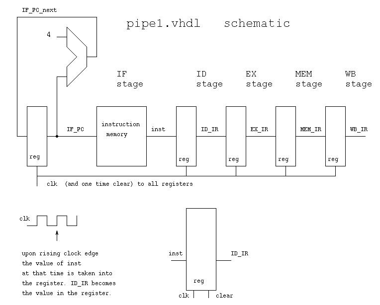 pipe1.vhdl implementation moves instruction
note clock and reset generation
look at register behavioral implementation
instruction memory is preloaded
pipe1.out just numbers used for demonstration
Pipelined Architecture with distributed control
pipe1.vhdl implementation moves instruction
note clock and reset generation
look at register behavioral implementation
instruction memory is preloaded
pipe1.out just numbers used for demonstration
Pipelined Architecture with distributed control
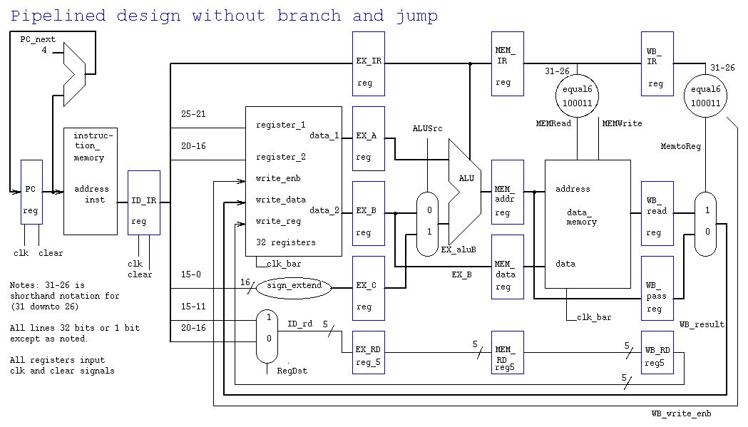 pipe2.vhdl note additional entities
equal6 for easy decoding
data memory behavioral implementation
pipe2.out instructions move through stages
pipe2.vhdl note additional entities
equal6 for easy decoding
data memory behavioral implementation
pipe2.out instructions move through stages
Timing analysis
Consider four instructions being executed.
First on the single cycle architecture, needing 8ns per instruction.
The time for each part of the circuit is shown.
The clock would be:
+---------------+ +---------------+ +------
| | | | |
-+ +---------------+ +---------------+
Single cycle execution 125MHZ clock
0 1 2 3 4 5 6 7 8 9 10 11 12 13 14 15 16 17ns
| | | | | | | | | | | | | | | | | |
+-------+---+-------+-------+---+
|IF |ID | EX | MEM |WB |
+-------+---+-------+-------+---+
+-------+---+-------+-------+---+
|IF |ID | EX | MEM |WB |
+-------+---+-------+-------+---+
+---
|IF ... 24ns
+---
... 32ns
The four instructions finished in 32ns.
An instruction started every 8ns.
An instruction finished every 8ns.
Now, the pipelined architecture has the clock determined by the slowest
part between clocked registers. Typically, the ALU. Thus use the same
ALU time as above, the clock would be:
+---+ +---+ +---+ +---+ +---+ +---+ +---+ +---+ +---+
| | | | | | | | | | | | | | | | | |
-+ +---+ +---+ +---+ +---+ +---+ +---+ +---+ +---+ +-
Pipelined Execution 500MHZ clock **
+-------+-------+-------+-------+-------+
|IF |ID reg| EX | MEM |reg WB |
+-------+-------+-------+-------+-------+
+-------+-------+-------+-------+-------+
|IF |ID reg| EX | MEM |reg WB |
+-------+-------+-------+-------+-------+
+-------+-------+-------+-------+-------+
|IF |ID reg| EX | MEM |reg WB |
+-------+-------+-------+-------+-------+
+-------+-------+-------+-------+-------+
|IF |ID reg| EX | MEM |reg WB |
+-------+-------+-------+-------+-------+
**
| | | | | | | | | | | | | | | | | |
0 1 2 3 4 5 6 7 8 9 10 11 12 13 14 15 16 17ns
The four instructions finished in 16ns. (But, the speedup is not 2)
An instruction started every 2ns.
An instruction finished every 2ns. Thus, the speedup is 8ns/2ns = 4 .
Since an instruction finishes every 2ns for the pipelined architecture and
every 8ns for the single cycle architecture, the speedup will be
8ns/2ns = 4. The speedup would change with various numbers of instructions
if the total time was used. Thus, the time between the start or end of
adjacent instructions is used in computing speedup.
Note the ** above in the pipeline. The first of the four instructions
may load a value in a register. This load takes place on the falling
edge of the clock. The fourth instruction is the earliest instruction
that could use the register loaded by the first instruction. The
use of the register comes after the rising edge of the clock. Thus use
of both halves of the clock cycle is important to this architecture and
to many modern computer architectures.
Remember, every stage of the pipeline must be the same time duration.
The system clock is used by all pipeline registers.
The slowest stage determines this time duration and thus determines
the maximum clock frequency.
The worse case delay that does not happen often because of optimizing
compilers, is a load word, lw, instruction followed by an instruction
that needs the value just loaded. The sequence of instructions, for
this unoptimized architecture, would be:
lw $1,val($0) load the 32 bit value at location val into register 1
nop
nop
addi $2,21($1) register 1 is available, add 21 and put result into reg 2
As can be seen in the pipelined timing below, lw would load register 1
by 9ns and register 1 would be used by addi by 10ns (**). The actual
add would be finished by 12 ns and register 2 updated sum by 15 ns (***).
+-------+-------+-------+-------+-------+
lw $1,val($0)|IF |ID reg| EX | MEM |reg WB |
+-------+-------+-------+-------+-------+
+-------+-------+-------+-------+-------+
nop |IF |ID reg| EX | MEM |reg WB |
+-------+-------+-------+-------+-------+
+-------+-------+-------+-------+-------+
nop |IF |ID reg| EX | MEM |reg WB |
+-------+-------+-------+-------+-------+
+-------+-------+-------+-------+-------+
addi $2,21($1) |IF |ID reg| EX | MEM |reg WB |
+-------+-------+-------+-------+-------+
** ***
| | | | | | | | | | | | | | | | |
0 1 2 3 4 5 6 7 8 9 10 11 12 13 14 15 16
ns
The pipeline for this course with branch and jump optimized:
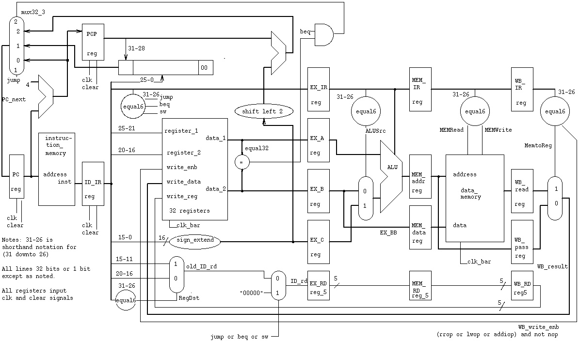 Note the three input mux replacing two mux in previous lecture.
Note the distributed control using the equal6 entity:
eq6j: entity WORK.equal6 port map(ID_IR(31 downto 26), "000010", jump);
cs411_opcodes.txt look at jump
In a later lecture, we will cover data forwarding to avoid nop's in
arithmetic and automatic stall to avoid putting all nop's in source code.
For the basic machine above, we have the timing shown here.
The branch slot, programming to avoid delays (filling in nop's):
Note: beq and jump always execute the next physical instruction.
This is called the "delayed branch slot", important for HW7.
if(a==b) x=3; /* simple C code */
else x=4;
y=5;
lw $1,a # possible unoptimized assembly language
lw $2,b # no ($0) shown on memory access
nop # wait for b to get into register 2
nop # wait for b to get into register 2
beq $1,$2,lab1
nop # branch slot, always executed *********
addi $1,4 # else part
nop # wait for 4 to get into register 1
nop # wait for 4 to get into register 1
sw $1,x # x=4;
j lab2
nop # branch slot, always executed *********
lab1: addi $1,3 # true part
nop # wait for 3 to get into register 1
nop # wait for 3 to get into register 1
sw $1,x # x=3;
lab2: addi $1,5 # after if-else, always execute
nop # wait for 5 to get into register 1
nop # wait for 5 to get into register 1
sw $1,y # y=5;
Unoptimized, 20 instructions.
Now, a smart compiler would produce the optimized code:
lw $1,a # possible unoptimized assembly language
lw $2,b # no ($0) shown on memory access
addi $4,4 # for else part later
addi $3,3 # for true part later
beq $1,$2,lab1
addi $5,5 # branch slot, always executed, for after if-else
j lab2
sw $4,x # x=4; in branch slot, always executed !! after jump
lab1: sw $3,x # x=3;
lab2: sw $5,y # y=5;
Optimized, 10 instructions.
The pipeline stage diagram for a==b true is:
1 2 3 4 5 6 7 8 9 10 11 12 clock
lw $1,a IF ID EX MM WB
lw $2,b IF ID EX MM WB
addi $4,4 IF ID EX MM WB
addi $3,3 IF ID EX MM WB
beq $1,$2,L1 IF ID EX MM WB assume equal, branch to L1
addi $5,5 IF ID EX MM WB delayed branch slot
j L2
sw $4,x
L1:sw $3,x IF ID EX MM WB
L2:sw $5,y IF ID EX MM WB
1 2 3 4 5 6 7 8 9 10 11 12
The pipeline stage diagram for a==b false is:
1 2 3 4 5 6 7 8 9 10 11 12 13 clock
lw $1,a IF ID EX MM WB
lw $2,b IF ID EX MM WB
addi $4,4 IF ID EX MM WB
addi $3,3 IF ID EX MM WB
beq $1,$2,L1 IF ID EX MM WB assume not equal
addi $5,5 IF ID EX MM WB
j L2 IF ID EX MM WB jumps to L2
sw $4,x IF ID EX MM WB
L1:sw $3,x
L2:sw $5,y IF ID EX MM WB
1 2 3 4 5 6 7 8 9 10 11 12 13
if(a==b) x=3; /* simple C code */
else x=4;
y=5;
Renaming when there are extra registers that the programmer can
not assess (diagram in Alpha below) with multiple units there can be
multiple issue (parallel execution of instructions)
The architecture sees the binary instructions from the following:
lw $1,a
lw $2,b
nop
sll $3,$1,8
sll $6,$2,8
add $9,$1,$2
sw $3,c
sw $6,d
sw $9,e
lw $1,aa
lw $2,bb
nop
sll $3,$1,8
sll $6,$2,8
add $9,$1,$2
sw $3,cc
sw $6,dd
sw $9,ee
Two ALU's, each with their own pipelines, multiple issue, register renaming:
The architecture executes two instruction streams in parallel.
(Assume only 32 user programmable registers, 80 registers in hardware.)
lw $1,a lw $41,aa
lw $2,b lw $42,bb
nop nop
sll $3,$1,8 sll $43,$41,8
sll $6,$2,8 sll $46,$42,8
add $9,$1,$2 add $49,$41,$42
sw $3,c sw $43,cc
sw $6,d sw $46,dd
sw $9,e sw $49,ee
Out of order execution to avoid delays. As seen in the first example,
changing the order of execution without changing the semantics of the
program can achieve faster execution.
There can be multiple issue when there are multiple arithmetic and
other units. This will require significant hardware to detect the
amount of out of order instructions that can be issued each clock.
Now, hardware can also be pipelined, for example a parallel multiplier.
Suppose we need to have at most 8 gate delays between pipeline
registers.
Note the three input mux replacing two mux in previous lecture.
Note the distributed control using the equal6 entity:
eq6j: entity WORK.equal6 port map(ID_IR(31 downto 26), "000010", jump);
cs411_opcodes.txt look at jump
In a later lecture, we will cover data forwarding to avoid nop's in
arithmetic and automatic stall to avoid putting all nop's in source code.
For the basic machine above, we have the timing shown here.
The branch slot, programming to avoid delays (filling in nop's):
Note: beq and jump always execute the next physical instruction.
This is called the "delayed branch slot", important for HW7.
if(a==b) x=3; /* simple C code */
else x=4;
y=5;
lw $1,a # possible unoptimized assembly language
lw $2,b # no ($0) shown on memory access
nop # wait for b to get into register 2
nop # wait for b to get into register 2
beq $1,$2,lab1
nop # branch slot, always executed *********
addi $1,4 # else part
nop # wait for 4 to get into register 1
nop # wait for 4 to get into register 1
sw $1,x # x=4;
j lab2
nop # branch slot, always executed *********
lab1: addi $1,3 # true part
nop # wait for 3 to get into register 1
nop # wait for 3 to get into register 1
sw $1,x # x=3;
lab2: addi $1,5 # after if-else, always execute
nop # wait for 5 to get into register 1
nop # wait for 5 to get into register 1
sw $1,y # y=5;
Unoptimized, 20 instructions.
Now, a smart compiler would produce the optimized code:
lw $1,a # possible unoptimized assembly language
lw $2,b # no ($0) shown on memory access
addi $4,4 # for else part later
addi $3,3 # for true part later
beq $1,$2,lab1
addi $5,5 # branch slot, always executed, for after if-else
j lab2
sw $4,x # x=4; in branch slot, always executed !! after jump
lab1: sw $3,x # x=3;
lab2: sw $5,y # y=5;
Optimized, 10 instructions.
The pipeline stage diagram for a==b true is:
1 2 3 4 5 6 7 8 9 10 11 12 clock
lw $1,a IF ID EX MM WB
lw $2,b IF ID EX MM WB
addi $4,4 IF ID EX MM WB
addi $3,3 IF ID EX MM WB
beq $1,$2,L1 IF ID EX MM WB assume equal, branch to L1
addi $5,5 IF ID EX MM WB delayed branch slot
j L2
sw $4,x
L1:sw $3,x IF ID EX MM WB
L2:sw $5,y IF ID EX MM WB
1 2 3 4 5 6 7 8 9 10 11 12
The pipeline stage diagram for a==b false is:
1 2 3 4 5 6 7 8 9 10 11 12 13 clock
lw $1,a IF ID EX MM WB
lw $2,b IF ID EX MM WB
addi $4,4 IF ID EX MM WB
addi $3,3 IF ID EX MM WB
beq $1,$2,L1 IF ID EX MM WB assume not equal
addi $5,5 IF ID EX MM WB
j L2 IF ID EX MM WB jumps to L2
sw $4,x IF ID EX MM WB
L1:sw $3,x
L2:sw $5,y IF ID EX MM WB
1 2 3 4 5 6 7 8 9 10 11 12 13
if(a==b) x=3; /* simple C code */
else x=4;
y=5;
Renaming when there are extra registers that the programmer can
not assess (diagram in Alpha below) with multiple units there can be
multiple issue (parallel execution of instructions)
The architecture sees the binary instructions from the following:
lw $1,a
lw $2,b
nop
sll $3,$1,8
sll $6,$2,8
add $9,$1,$2
sw $3,c
sw $6,d
sw $9,e
lw $1,aa
lw $2,bb
nop
sll $3,$1,8
sll $6,$2,8
add $9,$1,$2
sw $3,cc
sw $6,dd
sw $9,ee
Two ALU's, each with their own pipelines, multiple issue, register renaming:
The architecture executes two instruction streams in parallel.
(Assume only 32 user programmable registers, 80 registers in hardware.)
lw $1,a lw $41,aa
lw $2,b lw $42,bb
nop nop
sll $3,$1,8 sll $43,$41,8
sll $6,$2,8 sll $46,$42,8
add $9,$1,$2 add $49,$41,$42
sw $3,c sw $43,cc
sw $6,d sw $46,dd
sw $9,e sw $49,ee
Out of order execution to avoid delays. As seen in the first example,
changing the order of execution without changing the semantics of the
program can achieve faster execution.
There can be multiple issue when there are multiple arithmetic and
other units. This will require significant hardware to detect the
amount of out of order instructions that can be issued each clock.
Now, hardware can also be pipelined, for example a parallel multiplier.
Suppose we need to have at most 8 gate delays between pipeline
registers.
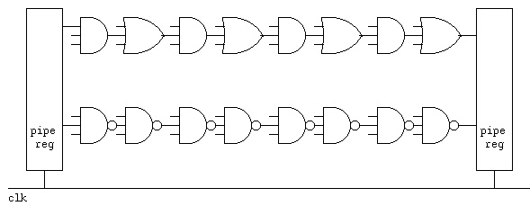 Note that any and-or-not logic can be converted to use only nand gates
or only nor gates. Thus, two level logic can have two gate delays.
We can build each multiplier stage with two gate delays. Thus we can
have only four multiplier stages then a pipeline register. Using a
carry save parallel 32-bit by 32-bit multiplier we need 32 stages, and
thus eight pipeline stages plus one extra stage for the final adder.
Note that any and-or-not logic can be converted to use only nand gates
or only nor gates. Thus, two level logic can have two gate delays.
We can build each multiplier stage with two gate delays. Thus we can
have only four multiplier stages then a pipeline register. Using a
carry save parallel 32-bit by 32-bit multiplier we need 32 stages, and
thus eight pipeline stages plus one extra stage for the final adder.
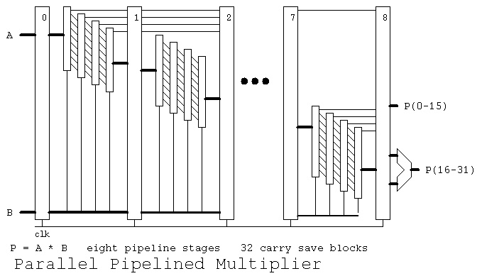 Note that a multiply can be started every clock. Thus a multiply
can be finished every clock. The speedup including the last adder
stage is 9 as shown in:
pipemul_test.vhdl
pipemul_test.out
pipemul.vhdl
A 64-bit PG adder may be built with eight or less gate delays.
The signals a, b and sum are 64 bits. See add64.vhdl for details.
Note that a multiply can be started every clock. Thus a multiply
can be finished every clock. The speedup including the last adder
stage is 9 as shown in:
pipemul_test.vhdl
pipemul_test.out
pipemul.vhdl
A 64-bit PG adder may be built with eight or less gate delays.
The signals a, b and sum are 64 bits. See add64.vhdl for details.
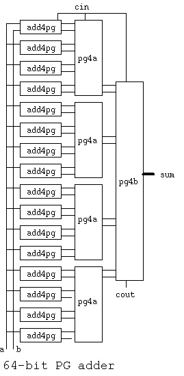 add64.vhdl
Any combinational logic can be performed in two levels with "and" gates
feeding "or" gates, assuming complementation time can be ignored.
Some designers may use diagrams but I wrote a Quine McClusky minimization
program that computes the two level and-or-not VHDL statement
for combinational logic.
quine_mcclusky.c logic minimization
eqn4.dat input data
eqn4.out both VHDL and Verilog output
Not as practical, I wrote a Myhill minimization of a finite state machine,
a Deterministic Finite Automata, that inputs a state transition table
and outputs the minimum state equivalent machine. "Not as practical"
because the design of sequential logic should be understandable. The
minimized machine's function is typically unrecognizable.
myhill.cpp state minimization
initial.dfa input data
myhill.dfa minimized output
A reasonably complete architecture description for the Alpha
showing the pipeline is:
basic Alpha
more complete Alpha
The "Cell" chip has unique architecture:
Cell architecture
Some technical data on Intel Core Duo (With some advertising.)
Core Duo all on WEB
From Intel, with lots of advertising:
power is proportional to capacitance * voltage^2 * frequency, page 7.
tech overview
whitepaper
Intel quad core demonstrated
AMD quad core
By 2010 AMD had a 12-core available and Intel had a 8-core available.
and 24 core and 48 core AMD
IBM Power6 at 4.7GHz clock speed
Intel I7 920 Nehalem 2.66GHz not quad $279.99
Intel I7 940 Nehalem 2.93GHz quad core $569.99
Intel I7 965 Nehalem 3.20GHz quad core $999.99
Prices vary with time, NewEgg.com search Intel I7
Motherboard Asus products-motherboards-intel i7
Intel socket 1366
Supermicro.com motherboards, 12-core
local, bad formatting, in case web page goes away. Good history.
Core Duo 1
Core Duo 2
Core Duo 3
Core Duo 4
Core Duo 5
Core Duo 6
Core Duo 7
Core Duo 8
add64.vhdl
Any combinational logic can be performed in two levels with "and" gates
feeding "or" gates, assuming complementation time can be ignored.
Some designers may use diagrams but I wrote a Quine McClusky minimization
program that computes the two level and-or-not VHDL statement
for combinational logic.
quine_mcclusky.c logic minimization
eqn4.dat input data
eqn4.out both VHDL and Verilog output
Not as practical, I wrote a Myhill minimization of a finite state machine,
a Deterministic Finite Automata, that inputs a state transition table
and outputs the minimum state equivalent machine. "Not as practical"
because the design of sequential logic should be understandable. The
minimized machine's function is typically unrecognizable.
myhill.cpp state minimization
initial.dfa input data
myhill.dfa minimized output
A reasonably complete architecture description for the Alpha
showing the pipeline is:
basic Alpha
more complete Alpha
The "Cell" chip has unique architecture:
Cell architecture
Some technical data on Intel Core Duo (With some advertising.)
Core Duo all on WEB
From Intel, with lots of advertising:
power is proportional to capacitance * voltage^2 * frequency, page 7.
tech overview
whitepaper
Intel quad core demonstrated
AMD quad core
By 2010 AMD had a 12-core available and Intel had a 8-core available.
and 24 core and 48 core AMD
IBM Power6 at 4.7GHz clock speed
Intel I7 920 Nehalem 2.66GHz not quad $279.99
Intel I7 940 Nehalem 2.93GHz quad core $569.99
Intel I7 965 Nehalem 3.20GHz quad core $999.99
Prices vary with time, NewEgg.com search Intel I7
Motherboard Asus products-motherboards-intel i7
Intel socket 1366
Supermicro.com motherboards, 12-core
local, bad formatting, in case web page goes away. Good history.
Core Duo 1
Core Duo 2
Core Duo 3
Core Duo 4
Core Duo 5
Core Duo 6
Core Duo 7
Core Duo 8
No comments:
Post a Comment